High-Reliability All-purpose Spring Finger
Product Applications
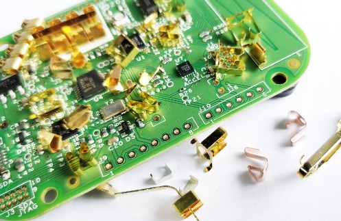
Grounding of All Kinds of Pcbs (mobile Phone And Communication Equipment)
Optical Elements
Grounding of Vehicle-mounted Mainboard
internal Construction Parts of Laptop
Shielding Can Fixing Or Wire Fixing
Precautions on Design of Grounding Spring Fingers
1: Methods of Product Fixing (welding, Screw, And Clip, Etc.)
2: Working Height And Design Height (involving the Elasticity of the Material And the Requirements of Its Use; Focusing on Assessing the Risk of Failure).
3: Working Environment Requirements And Corrosion Resistance (selecting Materials And Coatings)
4: Smt Automation Requirements (selection of Packaging Method And Design of Carrier Tape)
5: Operating Current And Voltage Used. (product Cross-sectional Area And Material Used)
6: Product Structural Space (structure Selection of the Spring Finger)
7: Product Reliability Test (such As Requirements on Compression Times And Compression Resilience)
Advantages of Smd Spring Finger
It Has High Reliability And Long Service Life, And Can Withstand High Temperature And High Humidity Environment.
Automated Production Greatly Reduces Its Labor Cost.
With Low Impedance, It Can Realize Good Emi&esd Effects.
Because of Its Good Formability, It Can Be Flexibly Designed And Used in All Kinds of Thin, Short Or Complex Mechanisms.
| FC@Part No. | Material | Plating | Scope of Application | Shape and Size |
|---|---|---|---|---|
| E-0013 | Stainless Steel | Gold Plating+Nickel Plating | 0.65~0.90 | 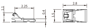 |
| E-0014 | Stainless Steel | Gold Plating+Nickel Plating | 0.45~0.70 | 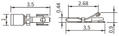 |
| E-0015 | Stainless Steel | Gold Plating+Nickel Plating | 1.0~1.6 | 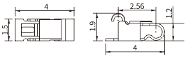 |
| E-0016 | Stainless Steel | Gold Plating+Nickel Plating | 1.6~2.3 | 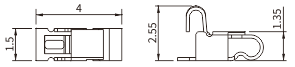 |
| E-0017 | Stainless Steel | Gold Plating+Nickel Plating | 2.2~3.0 | 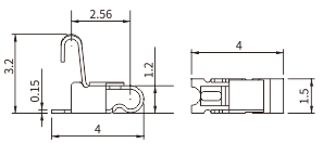 |
| E-0018 | Stainless Steel | Gold Plating+Nickel Plating | 2.3~3.5 | 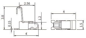 |
| E-0019 | Stainless Steel | Gold Plating+Nickel Plating | 0.8~1.2 | 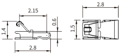 |
| E-0020 | Stainless Steel | Gold Plating+Nickel Plating | 1.4~1.7 | 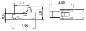 |